Indium antimonide (lnSb) is a promising semiconducting material that has been implemented in various electronic applications due to its high carrier mobility and carrier density. In particular, studies of lnSb nanowire clusters have yet to be explored in detail, despite the advantages of wire clusters can bring to the touch screen technologies and flexible devices. Therefore, the main focus of this thesis is to study the electronic transport properties within lnSb nanowire clusters such as schottky barrier height (SBH), conductivity, carrier density, and carrier mobility.
According to field emission scanning electron microscope-energy dispersive x-ray (FESEM-EDX) analysis, the clusters comprised of agglomerated, flowery-shaped nanowires and bulk lnSb, with stoichiometric 1 :1 ratio. The x-ray diffraction (XRD) analysis shows that the wire clusters exhibit polycrystalline nature, with several impurities present such as Sb, ln2O3, Sb2O3, and Al2O3. In order to study the electrical transport behaviours of lnSb nanowire clusters, two parameters, namely nanowire diameters and contact gap widths were chosen. For the effects of nanowire diameters, it was observed that most electronic transport properties such as conductivity (0.34 to 3.61 x 10⁻⁴ S/m), carrier density (7.41 to 7.49 x 1010 cm-3), and carrier mobility (0.48 to 4.82 x 10⁻¹⁵ cm2 V-1 s-1) increases with increasing diameters (20 to 200 nm). This is due to several reasons such as decreased grain boundaries and scattering effects, as well as increased electron charge density, thus allowing easier movement of carriers throughout the metalsemiconductor-metal (MSM) junction.
Meanwhile, SBH is shown to be inconsistent with increasing diameter, which is possibly because of the presence of lnSb bulk structure that might have influenced the electronic transport within the wire clusters. For the effects of contact gap width, most of the electronic transport properties such as conductivity (1.67 to 4.58 x 10⁻⁵ S/m), carrier density (7.41 to 7.45 x 1010 cm-3), and carrier mobility (0.23 to 0.61 x 10⁻¹⁵ cm2 V-1 s-1) were shown to increase with decreasing gap size (343.07 to 277.72 µm), while SSH decreases (0.68 to 0.66 eV). This is because of the closer distribution within nanowire clusters when the gap width decreases, and hence improving the current transport throughout the MSM junction. Due to several factors such as presence of defects and less compact distribution compared to particle arrangements within bulk structure, thin film and single nanowire, nanowire clusters exhibit lower electronic transport properties. Nevertheless, further investigations on the semiconductor nanowire clusters will open more opportunities to discover its potentials in a wide variety of electronic components in the future.
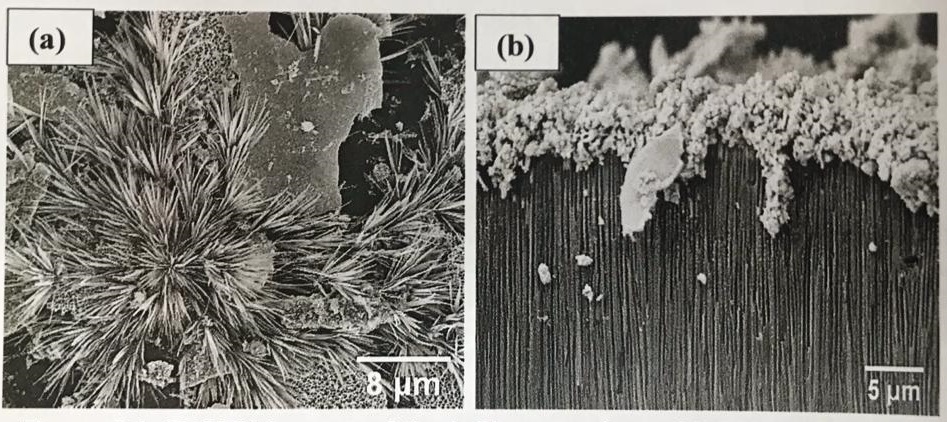
Figure 5.1: FESEM images of the lnSb nanowires with 200 nm diameter.
*Abstract of the thesis (Master) by Intan Nur Ain bt Arifin @ Mohd Ripin
For further information please contact:
Dr. Suriati binti Paiman, PhD
Chairman
suriati@upm.edu.my
Date of Input: 26/01/2022 | Updated: 26/01/2022 | roslina_ar
MEDIA SHARING