Zinc oxide (ZnO) nanorods have shown great potential in various applications such as gas sensing, photocatalysis, and piezoelectric nanogenerators. Thus, it is crucial to investigate the growth orientation, morphology and properties of ZnO nanostructures for aformentioned applications. The work focused on the nanoscale domain imaging and the electromechanical response of ZnO nanorod arrays synthesized process involved the use of a simple and low-cost hydrothermal method on different substrates, followed by the fabrication and characterization of optimized ZnO nanostructured on printed microcontact electrode.
This simple and cost-effective hydrothermal method involves the growth of ZnO nanorods on a substrate through the reaction between zinc nitrate hexahydrate and hexamethylenetetramine in a basic solution. The advantageous is because of the relatively simple and requires minimal equipment and expertise, making it a cost-effective option for large-scale production. The use of a printed microcontact electrode also provided a cost-effective approach to fabricating the nanorod arrays with a high degree of uniformity (Figure 1). This approach allowed for the precise control of the nanorod growth and alignment, which is important for the piezoelectric performance of the arrays.
We then investigated their piezoelectric properties using various techniques such as scanning electron microscopy (SEM), X-ray diffraction (XRD), and piezoresponse force microscopy (PFM) (shown in Figure 2).
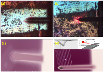
Figure 1. Schematic of conventional AFM set-up used in PFM-measurements with both AC and DC voltages are applied to the conductive tip and the resulting electromechanical response of the nanorods is measured.
The SEM images revealed that the ZnO nanostructures were uniform in shape and well-aligned on glass, silicon and the printed microcontact electrode. The XRD patterns confirmed the crystalline structure of the ZnO nanostructures, which was found to be wurtzite.
Using this PFM and atomic force microscopy (AFM), we were able to observe the nanoscale electromechanical response and map out the piezoelectric domains (Figure 3) of the nanorods. We found that the domain size and distribution were influenced by the choice of substrate and that the Young's modulus of the nanorods was dependent on their orientation and aspect ratio. The ZnO nanostructures/nanorod arrays exhibited a high piezoelectric response, which was attributed to their uniform polarization distribution. Additionally, the impedance analysis showed that the ZnO nanostructures had a high impedance, which was indicative of their piezoelectric properties. The AFM measurements also indicated that the ZnO nanorod arrays had a high piezoelectric response, which varied depending on the substrate. Specifically, the ZnO nanorod arrays grown on silicon showed a higher piezoelectric response compared to those grown on glass.
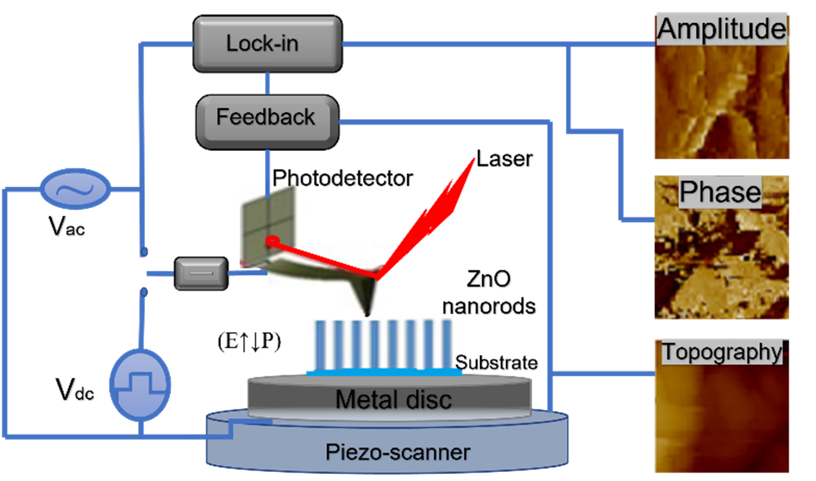
Figure 2. (a) Hysteresis curves for the PFM Phase and (b) PFM Amplitude signal. A phase switch of the response and hysteresis in phase vs. dc voltage plot is known as an evidence of local polarization switching indicating ferroelctricity, whereas, hysteresis in amplitude with field indicates piezoelectric behavior.
The SEM images revealed that the ZnO nanostructures were uniform in shape and well-aligned on glass, silicon and the printed microcontact electrode. The XRD patterns confirmed the crystalline structure of the ZnO nanostructures, which was found to be wurtzite.
Using this PFM and atomic force microscopy (AFM), we were able to observe the nanoscale electromechanical response and map out the piezoelectric domains (Figure 3) of the nanorods. We found that the domain size and distribution were influenced by the choice of substrate and that the Young's modulus of the nanorods was dependent on their orientation and aspect ratio. The ZnO nanostructures/nanorod arrays exhibited a high piezoelectric response, which was attributed to their uniform polarization distribution. Additionally, the impedance analysis showed that the ZnO nanostructures had a high impedance, which was indicative of their piezoelectric properties. The AFM measurements also indicated that the ZnO nanorod arrays had a high piezoelectric response, which varied depending on the substrate. Specifically, the ZnO nanorod arrays grown on silicon showed a higher piezoelectric response compared to those grown on glass.
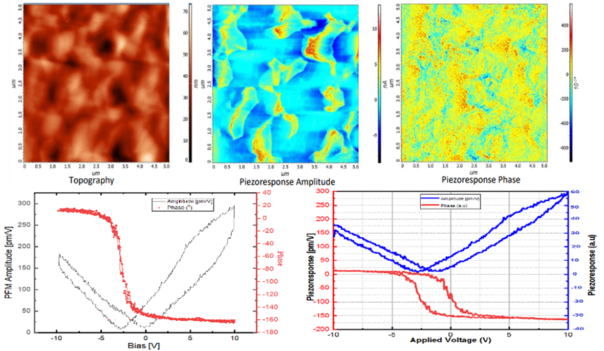
Figure 3. (a) Hysteresis curves for the PFM Phase and (b) PFM Amplitude signal. A phase switch of the response and hysteresis in phase vs. dc voltage plot is known as an evidence of local polarization switching indicating ferroelctricity, whereas, hysteresis in amplitude with field indicates piezoelectric behavior.
These findings have important implications for the design and fabrication of nanorod arrays for sensing and energy harvesting applications through the precise control of the nanorod growth and alignment, which is important for the piezoelectric performance of the arrays.
DOI:10.1016/j.jmrt.2021.07.125
DOI:10.1016/j.jmrt.2020.11.038
ASSOC. PROF. TS. DR. SURIATI PAIMAN
Research Associate
Functional Nanotechnology Devices Laboratory (FNDL)
Institute of Nanoscience and Nanotechnology, UPM
suriati@upm.edu.my
Date of Input: 31/03/2023 | Updated: 10/08/2023 | roslina_ar
MEDIA SHARING